A friend and co-worker on a large telescope camera project (he asked to remain anonymous), had the following to say:
"If it's only seen when 656nm light shines on the sensor, and if there's no cover glass, there must be an etalon effect within the sensor itself. At wavelengths where the silicon is semi-transparent (more precisely, when the absorption length is longer than the thickness) the light reflected from the front and back silicon-air interfaces interferes to create standing wave intensity patterns depending on the local thickness -- i.e. constructive interference when the optical thickness is an integer multiple of the wavelength. For polychromatic , broadband light these patterns wash out. It's similar to the Newton's ring patterns on oil films.
Our sensors show complicated fringing patterns when illuminated with narrowband light at wavelengths >930nm. For a long time we attributed this to reflections between the silicon front and back interfaces, but recent analysis showed it is actually comprised of two patterns overlaid. One is from the silicon front-back side, but the more prominent one seems to be coming from the layer of epoxy where the silicon is glued to a support structure. In your sensor it's possible that there is a similar non-silicon layer whose thickness, and thickness variation, conspire to produce an interference having the structured pattern you see. In that case one would need to know the optical properties (refractive index and absorption length at 656nm) as well as the thickness to get a sense of the thickness variation that could produce that pattern. Since there's no fringe-like pattern, it would have to mean that the thickness variation is never more than one wavelength.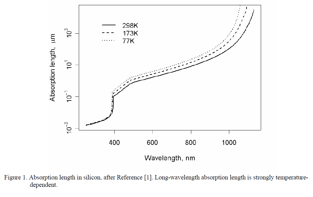
Here's the absorption length vs. wavelength and temperature for silicon for reference. If you know the QE at H-a (and reflection losses) you can estimate whether the silicon is transparent enough for it to be a silicon etalon effect."
So my hypothesis was close, in that I attributed it to underlying structure (which could be the adhesive, as he points out).
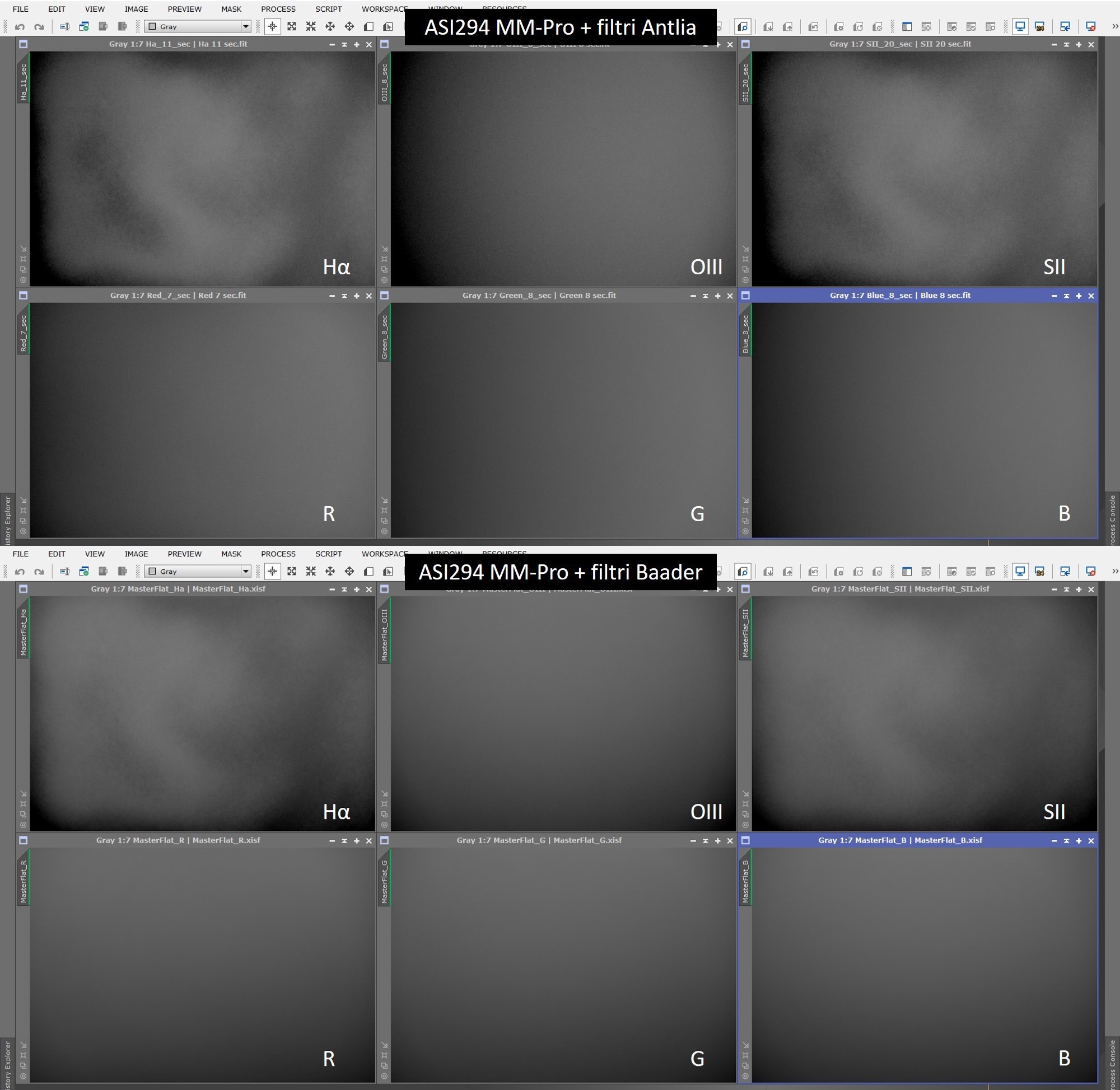
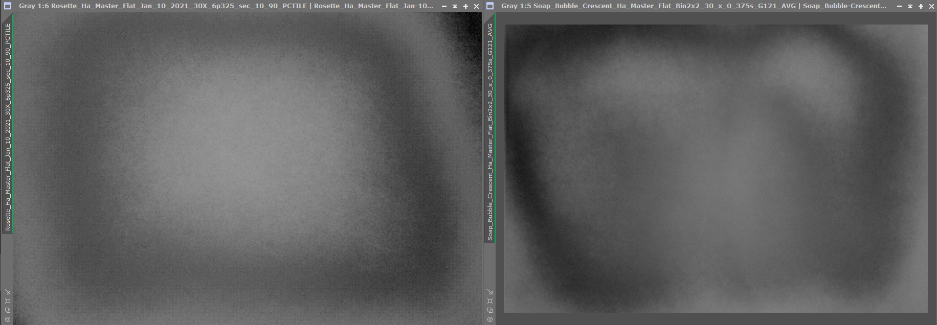
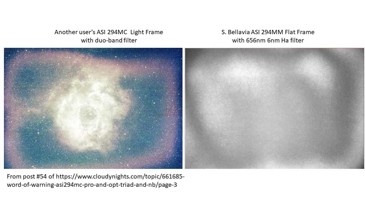
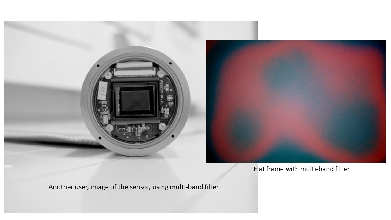
I believe this, or at least something very similar, is the cause of these patterns in Ha and Sii wavelengths.
Note: I just tried sodium (589nm @10nm bandwidth) and a long-pass, 685nm filter, and neither show the pattern. So, apparently 589nm is too short, and It will not show up in broad bandwidths, respectively. The thickness of the silicon and/or adhesive must be around 650 to 680nm, or an integer multiple of that, as it only shows up in Ha and SII light.
Steve